10 ENGLISH BOOKS RELATING TO «NAND GATE»
Discover the use of
NAND gate in the following bibliographical selection. Books relating to
NAND gate and brief extracts from same to provide context of its use in English literature.
1
CMOS: Circuit Design, Layout, and Simulation
Example 12.3 Estimate the intrinsic propagation delays, tPHL + tPLH, of a three-
input NAND gate made using 10/1 NMOS and 20/1 PMOS in the short-channel
process. Estimate and simulate the delay when the gate is driving a load ...
2
Digital Design with CPLD Applications and VHDL
We must keep in mind that a NAND gate combines all of its inputs in an AND
function, then inverts the total result. Similarly, a NOR combines all of its inputs in
an OR function, then inverts the result. Therefore, inversion must not be done
until ...
3
Classical and Quantum Computing: With C++ and Java Simulations
With C++ and Java Simulations Yorick Hardy. 4.2.5 NAND Gate The NAND gate
is an AND gate followed by an inverter. A NAND gate can have two or more
inputs. Thus the NAND gate is formed by appending NOT to AND. The output will
be ...
4
Digital Design with RTL Design, Verilog and VHDL
To implement a NOT gate using NAND gates, we can substitute the NOT gate
with a two-input NAND gate having its two inputs tied together, as shown in
Figure 7.8. The truth table in the figure shows that the NAND gate with its inputs
tied ...
5
Computer Logic: Design Principles and Applications
Where low voltage is concerned, the NAND gate provides the OR function.
Henceforth, a two-input NAND gate can be replaced by two inverters and a two-
input OR gate, as shown in Figure 4.3(c). An IC chip may contain four two-input
NAND ...
6
Competition Science Vision
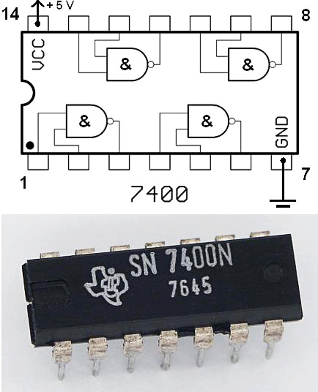
gate (fig. a), the resulting gate is called NAND gate. The logic symbol of NAND
gate is shown in fig. (b). NAND Gate AND gate NOTGate (b) The Boolean
expression for NAND gate is A.B = Y read as 'A AND B negated equals Y' Truth
Table of ...
7
Introduction to System Design Using Integrated Circuits
4.7.7 Special-Purpose Gates Typical special-purpose gates having a wide range
of applications are Schmitt- input NAND gate, AOI and expander gate and EX-OR
gate. Some aspects of these circuits are covered here. Schmitt-Input NAND ...
8
Digital Design and Computer Organization
FIGURE 3.6.1 Example Circuit Used to Derive NAND-NAND Design 3.6.1 NAND
Gate Design For the NAND gate design, we discuss the procedure by the
example circuit of a two-level AND-OR design, as shown in Figure 3.6.1. The
gate ...
9
Electronics, 2nd Edition
5.5.4 NAND gate representation The Boolean expressions for the outputs of the
BCD-to-seven-segment decoder could be implemented using the standard sum-
of-products circuit. The implementation therefore requires several AND, OR and ...
David Crecraft, David Gorham, 2003
10
Fundamentals of Logic Design
Figure 7-8(a) shows a three-input NAND gate. The small circle (or “bubble”) at
the gate output indicates inversion, so the NAND gate is equivalent to an AND
gate followed by an inverter, as shown in Figure 7-8(b). A more appropriate name
...
Charles Roth, Jr., Larry Kinney, 2013
10 NEWS ITEMS WHICH INCLUDE THE TERM «NAND GATE»
Find out what the national and international press are talking about and how the term
NAND gate is used in the context of the following news items.
New report shares details about the Global nand flash market that is …
In NAND flash, the cells are connected in a series that resembles a NAND gate. "Global NAND Flash Market 2015-2019" About NAND Flash:. «WhaTech, Jun 15»
Nanoplasmonic waveguides: towards applications in integrated …
Because the basic components (NW-based laser, BUS router, switch, adder, NAND gate) are already available, the future of nanophotonics is ... «Nature.com, Jun 15»
Memory Design At 16/14nm
As an example, Saggurti says, “In CMOS we were taught not to have more than four transistors stacked together, so a four-input NAND gate ... «SemiEngineering, May 15»
NRZ to AMI converter uses single supply
The NAND gate is used on the second line to obtain an inverted waveform (Figure 2c). Figure 1 The NRZ to AMI converter generating bipolar ... «EDN.com, Mar 15»
Add a dash of quantum for secure cloud computing
The sever can then perform a quantum measurement on the cobit in order to run a more powerful computation, called a NAND gate. In theory ... «New Scientist, Feb 15»
Design for test boot camp, part 1: Scan test
For example, if a NAND gate in the design had an input pin shorted to ground (logic value 0) by a defect, the stuck-at-0 test for that node would ... «EDN.com, Oct 14»
Researchers build first 3D magnetic logic gate
The input magnet in the third dimension also programs the gate to operate as either a NOR or NAND gate. NML has several potential ... «Phys.Org, Aug 14»
Pulleys As Logic Gates
All you need to build a computer is lots of NAND gate. Now take a look a the video where Alex Gorischek demonstrates how a set of ropes and ... «iProgrammer, Jun 14»
SanDisk - Offering Handsome Upside Potential
The design of NAND flash memory chips connected in a series bear a resemblance to a NAND gate. This allows the series connection to use ... «Seeking Alpha, May 14»
Moore's Law: The rule that really matters in tech
If you want to build a NOR gate or NAND gate [two forms of basic logic gates out of which chips are assembled], you need to switch from ... «CNET, May 14»