MOTS EN ANGLAIS EN RAPPORT AVEC «PHOTOLITHOGRAPHY»
photolithography
mask
steps
process
fabrication
history
basics
jobs
what
used
photolithography
also
termed
optical
lithography
microfabrication
pattern
parts
thin
film
bulk
substrate
uses
light
transfer
geometric
transferring
shapes
surface
silicon
involved
cymer
which
semiconductor
circuitry
patterned
wafers
source
provides
deep
ultraviolet
whatis
standard
method
printed
circuit
board
microprocessor
make
conductive
paths
angela
young
describes
background
shows
step
print
processes
capabilities
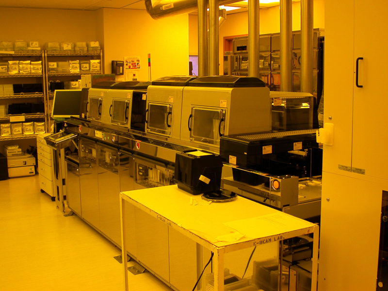
cornell
nanoscale
science
technology
facility
served
research
community
more
than
years
subjects
encompass
britney
spears
literally
meaning
stone
writing
greek
patterns
defined
using
instruments
products
newport
corporation
oriel
long
addressed
need
high
resolution
sources
this
began
advanced
design
mercury
define
electronics
whereby
produced
photographing
photosensitive
chemically
merriam
webster
thog
noun
ˈthä
grə
photographically
prepared
plates
nova
litho
projecting
microscopic
onto
involves
multiple
chemicals
materials
adhesion
page
10 LIVRES EN ANGLAIS EN RAPPORT AVEC «PHOTOLITHOGRAPHY»
Découvrez l'usage de
photolithography dans la sélection bibliographique suivante. Des livres en rapport avec
photolithography et de courts extraits de ceux-ci pour replacer dans son contexte son utilisation littéraire.
1
Double-exposure Gray-scale
Photolithography
The objective of this work is to investigate and evaluate a significant improvement
to the pixelated gray-scale photolithography process. This chapter provides the
background on pixelated gray-scale technology, including the two primary ...
Variation of gamma with developing time. straight-line portion. When making
continuous-tone negatives for photolithography, allowance must be made for the
slight loss of tone in the shadows, which takes place on making the halftone
positive ...
3
Surface Patterning of Biodegradable Polymer in Tissue ...
3.1.1 Patterning with Photolithography In the photolithography process,
geometric features drawn on a mask are transferred via UV illumination onto a
substrate. A mask is generally made of a quartz (glass) plate coated with a thin
layer of ...
4
Fundamentals of Microfabrication: The Science of ...
Today, photolithography, x-ray lithography, and charged-particle lithography all
achieve submicron printing accuracy. The Coppermine Pills chip from Intel (
introduced in late 1999), for example, incorporates a 0.18 urn minimum feature
size ...
5
Encyclopedia of nineteenth-century photography: A-I, index
Pouncy referred to the process used as photolithography but the images are
heavily retouched and Pouncy may have meant that the original photography
was manually copied by lithography that was in turn photolithographed. In the
same ...
6
MEMS & Microsystems: Design, Manufacture, and Nanoscale ...
According to Ruska (1987), the photolithography process involves the use of an
optical image and a photosensitive film to produce a pattern on a substrate.
Photolithography is one of the most important steps in microfabrication. It appears
to ...
7
Microengineering, MEMS, and Interfacing: A Practical Guide
1. Photolithography. 1.1 INTRODUCTION The fundamental aim of
microengineering — to take a design from a computer aided design (CAD)
software package and manifest it in a physical manner — may be achieved
through one of a number ...
8
Solid State and Quantum Theory for Optoelectronics
Photolithography and material deposition require baking the wafer above the
vapor point of the solvents to remove any residual moisture. The wafer is placed
in a convection oven at 1008C–1508C for at least 30 min and commonly up to 8
h.
9
Modern Physical Organic Chemistry
We begin with a basic overview of the process, and then discuss separately the
kinds of chemistries involved in negative and positive photoresists. 17.6.1
Photolithography Photolithography involves an optical process that imprints a
pattern ...
Eric V. Anslyn, Dennis A. Dougherty, 2006
10
Lab on a Chip Technology: Fabrication and microfluidics
μPLAT can be used to quickly fabricate low-cost lab-on-a-chip devices that
contain features that are difficult to achieve using photolithography-based
methods. For applications with resolution requirements above 50 μm, functioning
devices ...
K. E. Herold, Avraham Rasooly, 2009
10 ACTUALITÉS CONTENANT LE TERME «PHOTOLITHOGRAPHY»
Découvrez de quoi on parle dans les médias nationaux et internationaux et comment le terme
photolithography est employé dans le contexte des actualités suivantes.
Company Shares of Ultratech, Inc. Drops by -8.68%
The Company supplies step-and-repeat photolithography systems based on one-to-one (1X) imaging technology to customers located throughout North ... «OTC Outlook, juil 15»
History of photography in Ottoman Empire documented in İstanbul …
... Development of Photolithography,” and Öztuncay's text on the origins and development of photography in İstanbul. Eldem's “Powerful Images ... «Today's Zaman, juil 15»
New report shares details about the roll to roll technologies for …
... the advancements in battery design, chips and circuits. A technique called photolithography has shrunk the size of circuits nearly 400 times. «WhaTech, juil 15»
Ultratech (UTEK) Scheduled to Post Earnings on Thursday
The Company supplies step-and-repeat photolithography systems based on one-to-one (1X) imaging technology. It offers two different series of ... «sleekmoney, juil 15»
Ultratech (UTEK) to Release Earnings on Thursday
The Company supplies step-and-repeat photolithography systems based on one-to-one (1X) imaging technology. It offers two different series of ... «Dakota Financial News, juil 15»
Company Shares of Ultratech, Inc. Drops by -6.97%
Ultratech, Inc. (Ultratech) develops, manufactures and markets photolithography, laser thermal processing, and inspection equipment. «American Trade Journal, juil 15»
Moore's law hits a bump as Intel pushes back 10nm move
... 1975 prediction that transistor density would double every two years thanks to scaling advances that are largely a result of photolithography, ... «Optics.org, juil 15»
Huge business opportunities in the advanced packaging market are …
Within the photolithography equipment market reaching US150$M 2014 (Source: Photolithography Equipment & Materials for Advanced ... «Global LEDs/OLEDs, juil 15»
Understanding Polarization and Optical Coatings
DSI's photolithography production line is capable of patterning up to 200 mm diameter wafers, including populated wafers containing active devices. Patterning ... «Laser Focus world, juil 15»
ECC creating programs for renewable energy jobs
Techniques taught in the nanotechnology program include reactive ion etching, metallization and photolithography. ECC is also creating a ... «WKBW-TV, juil 15»